
Cactus Materials

Foundry // Services & Capabilities

Foundry services

Custom manufacturing and production services across our Silicon Carbide and III-V compound-semiconductor fabs — with wafer and packaging process services to support both R&D and production demands.

01 — Overview

Two fabs, full-service support

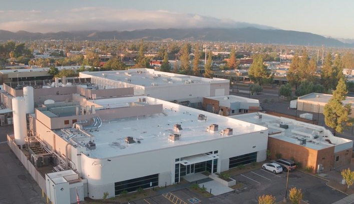
Cactus Materials runs two semiconductor fabs totaling 40,000 sq ft in Tempe, Arizona — a Silicon Carbide (SiC) fab for high-power devices and a III-V compound-semiconductor fab for AI photonics. We bring extensive fab experience across many markets, and provide wafer and packaging process services to support R&D and production.

02 — Fab capabilities

State-of-the-art process capability

Compound Semiconductor Epitaxial Fab

Precision epitaxial growth for III-V compound-semiconductor devices.

Wafer size up to 200 mm

Silicon Carbide High-Voltage / High-Temp Devices

SiC device fabrication for high-voltage, high-temperature power applications.

Wafer size up to 150 mm

03 — What we offer

Foundry & process services

Custom Manufacturing

Precision engineering for specialized, application-specific devices.

Production Services

Scalable, high-volume manufacturing on mature platforms.

Wafer Process Services

Epitaxial growth and wafer processing for R&D and production.

Packaging Support

Advanced packaging solutions — including wafer bonding, chip-level bare die, TO247, SOT227, and custom packaging — with partner support from prototype to production.

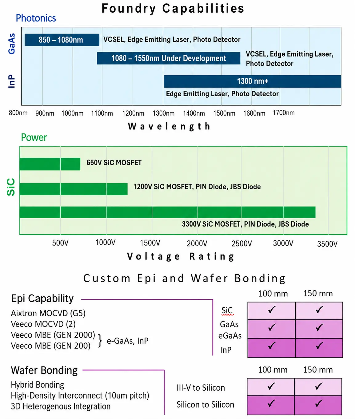
Foundry Capabilties

Photonics, Power, and Custom Epi capabilities across GaAs, eGaAs, InP, and SiC platforms - from 650V to 3300V, 850nm to 1700nm.
Foundry Capabilities
Silicon Carbide Fab III-V Compound Fab Wafer Process Services Custom Packaging ITAR Registered

Ready to discuss your manufacturing requirements?