Strategic Services
Our main business is designing & manufacturing our own products as an Integrated Device Manufacturer.
Key Capabilities
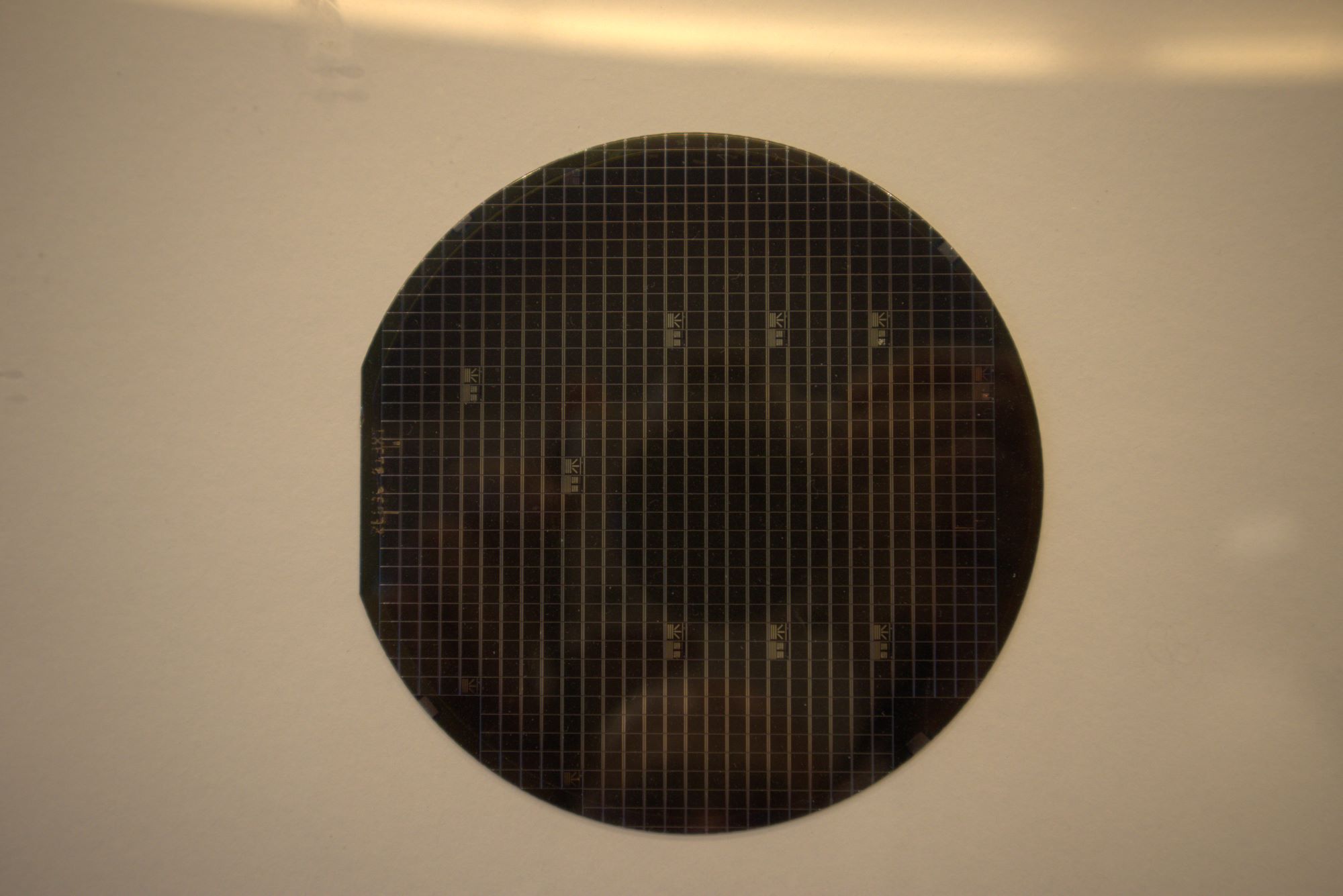
- State-of-the-art Compound Semiconductor Epitaxial fab (up-to 200 mm)
- 3D AI Optical Chip Integration and Packaging fab through wafer bonding (up-to-200 mm)
- Silicon Carbide (SiC) High Voltage and High Temperature Devices (up-to-150 mm)

SiC Silicon Carbide Foundry Services (30% of the Fab Capacity maximum)
This is just placeholder text. Don’t be alarmed, this is just here to fill up space since your finalized copy isn’t ready yet. Once we have your content finalized, we’ll replace this placeholder text with your real content.

III-V Epitaxy Wafer Development
This is just placeholder text. Don’t be alarmed, this is just here to fill up space since your finalized copy isn’t ready yet. Once we have your content finalized, we’ll replace this placeholder text with your real content.

Heterogenous 3D Integration (W2W) Wafter-To-Wafer
This is just placeholder text. Don’t be alarmed, this is just here to fill up space since your finalized copy isn’t ready yet. Once we have your content finalized, we’ll replace this placeholder text with your real content.

*Rad-Hard” Radiation Hardened* engineered Silicon Substrate
This is just placeholder text. Don’t be alarmed, this is just here to fill up space since your finalized copy isn’t ready yet. Once we have your content finalized, we’ll replace this placeholder text with your real content.

Key Equipment
- State-of-the-art 40,000 sq. ft
- Class 100 clean room
- 100+ pieces of advanced equipment and tools

